

Avago 公司的ALM-1912 是GPS" title="GPS">GPS前端模塊" title="前端模塊">前端模塊,包括有GPS FBAR濾波器和高增益低噪音放大器(LNA" title="LNA">LNA). ALM-1912具有非常低的噪音和極好Cell/PCS/WLAN頻帶抑制,在1.575GHz,Vdd = 2.7V和Idd = 6mA時,增益為19.3 dB, NF = 1.62 dB, IIP3 = +1.5 dBm,IP1dB = -8 dBm,主要用作GPS前端模塊.本文介紹了ALM-1912主要特性和指標, 應用電路, 演示和應用電路元件表以及演示和應用電路框圖與S參數(shù)測量參考平面.
Avago Technologies’ALM-1912 is a GPS front-end module that combines a GPS FBAR filter with high-gain low-noise amplifier (LNA).The LNA uses Avago Technologies’ proprietary GaAs Enhancement-mode pHEMT process to achieve high gain with very low noise figure and high linearity. Noise figure distribution is very tightly controlled.
A CMOS-compatible shutdown pin is included either for turning the LNA on/off or for current adjustment. The filter use Avago Technologies’ leading-edge FBAR filter for low GPS band insertion loss and exceptional rejection at Cellular, PCS and WLAN band frequencies.
The low noise figure and high gain, coupled with low current consumption make it suitable for use in critical low-power GPS applications or during low-battery situations.
ALM-1912主要特性:
Very Low Noise Figure
Exceptional Cell/PCS/WLAN-Band rejection
Low external component count
Fully-matched at RF input and RF output
Shutdown current : < 1 uA
CMOS compatible shutdown pin (SD)
ESD : > 3kV at RFin pin
2.9 x 2.0 x 0.95 mm size
Adjustable bias current via single external resistor/voltage
Lead-free and Halogen free
Specifications (Typical performance @ 25℃)
At 1.575GHz, Vdd = 2.7V, Idd = 6mA
Gain = 19.3 dB
NF = 1.62 dB
IIP3 = +1.5 dBm
IP1dB = -8 dBm
S11 = -9.5 dB
S22 =-13.5 dB
Cell-Band Rejection: > 57dBc
PCS-Band Rejection: > 53dBc
WLAN-Band Rejection: > 52dBc
ALM- 1912應用:
GPS Front-end Module

圖1.ALM-1912應用電路

圖2.ALM-1912演示和應用電路元件表
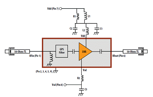
圖3.ALM-1912演示和應用電路框圖
Notes
The module is fully matched at the input and output RF pins. Both these pins also have built-in coupling and DC-blocking capacitors. Best noise performance is obtained using high-Q wirewound inductors. This circuit demonstrates that low noise figures are obtainable with standard 0402 chip inductors.
C2 and L2 form a matching network that affects the frequency response and linearity of the LNA, these can be tuned to optimize gain and return loss.
L1 and R1 isolates the demoboard from external disturbances during measurement. It is not needed in actual application. Likewise, C1 and C3 mitigate the effect of external noise pickup on the Vdd and Vsd lines respectively. These components are not required in actual operation.
Bias control is achieved by either varying the Vsd voltage with/without R2, or fixing the Vsd voltage to Vdd and adjusting R2 for the desired current.
R2 = 4.7Kohm will result 6mA when Vdd = Vsd = 2.7V. R2 = 2.7Kohm for 4mA when Vdd = Vsd = 1.8V & R2 = 15Kohm for 4mA when Vdd = Vsd =2.8V.

圖4.ALM-1912 S參數(shù)測量參考平面